Huskey's 12-Bit ACE Evaluator
Rainer Glaschick, Paderborn (rainer@glaschick.de)
2020-11-17
In 1964, Harry D. Huskey has published (chapter 6 in [Huskey1984]) his design for a extremely small variant of Turing's Automatic Computing Engine (ACE):
This was the simplest design I could work out using Turing's ideas.
… very restrictive and … unsuitable for general computation,
but it was sufficient to illustrate the principles.
Even if an operational version of the Pilot ACE would be available, a small educational model like Huskey's 12-bit ACE would have several benefits; it could be used to
- explain how Turing's ACE worked,
- build corresponding hardware, at least partially with valves.
Using documentation about Turing's ACE, the hardware according to the schematics could be built and used as a showpiece for the economy of Turing's solutions.
Unfortunately, Huskey did not provide any example programs in the document, because even very simple programs using the data delay lines are impossible.
Note that the relay-based machine named ACE Simulator (by Mike Woodger,
see [Woodger]) is not programmable, but still useful to demonstrate
the basic concept of a serial computer.
The original exists in the Science Museum, archive number 1951-164,
and should still be operable.
An educational re-built version should add a manual sequencer
instead of changing cable connections, as shown in my running model
of a decimal relay computer,
the MERAC (Mechano-Electrical Retrograde Automatic Computer),
which is a hybrid between Babbages Analytical Engine and the ENIAC.
As the length of the delay lines, i.e. the number of bits, is not a cost factor (only the clock ring counter and the input and output circuitry), a 16-bit variant would allow to have separate timings for data and instructions, and thus show the working of the ACE much more realistic; 32 instructions are more than enough.
Architecture
The term ACE generally refers to the Pilot ACE, while Huskey's design is coined the ACE-12H.
The Pilot ACE
The ACE (see e.g. [Wilkinson1951]) uses delay lines as memory for data (numbers) and instructions. It is a bit-serial architecture, with a 1 MHz bit clock and 32µs word cycle time. A long delay line (DL) has a capacity of 1024 bits, i.e. 32 words with 32 bits each. To access a word, the system has to wait until the first (lowest order) bit is available. A short or temporary delay line (TS) has just 32 bits, thus its contents is available without delay in every cycle.
Each instruction denotes a source and destination port, and in each non-wait cycle, 32 bits from the source port are sent to the destination port. Arithmetic, logical and other functions are mapped to specific source and destination ports; several ports are different views of the same memory. Although the pair of source and destination could be seen as an instruction code, part of the memory address of the data word and instruction is part of this value.
Instructions are not executed in any natural order; instead, the location of the next instruction is coded in the instruction word. This allows to avoid delays waiting for the next instruction or data to emerge from storage, but also makes programming rather complicated.
Selecting words in the long delay lines requires to wait until the word emerges, while short delay lines just rotate their content.
The very economical solution in the Pilot ACE — and this is what
the ACE-12H is designed to show — is to use a circulating
delay line for the current instruction,
and to modify this single register by subtracting one
from the timing fields W and T in each cycle.
If W to zero, the data transfer from
source to destination takes place, and when after that T
becomes zero, the next instruction is due.
The ACE-12H
Basis for the following description is [Huskey1984], not the derived later version that was published in [Huskey2005] and contains small errors and omissions.
The ACE-12H has a word length of 12 instead of 32 bits. It has two long delay lines, one for data and one for instructions, plus a short delay line as an accumulator. Another short one is used as an instruction register, which also serves as a counter for the wait time, as in the Pilot ACE.
There is only one instruction:
copy source (x) to destination (y) and skip the next (w) instructions
Sources and Destinations
The sources and destinations are (Table from [Huskey1984]):
| No. | Source | Destination | Special | Remarks |
|---|---|---|---|---|
| 0 | Input | Output | ||
| 1 | DL | DL | One long delay line (data) | |
| 2 | TS&P12 | TS | Sign bit, accumulator | |
| 3 | TS | +TS | Bell | Accumulator, add |
| 4 | P6 | Special | Read | |
| 5 | P1 | DL2 | Punch | 1 |
| 6 | DL2 | Instructions | D = instruction register | |
| 7 | I/O ready | — |
DL is the long delay line for data, TS the short delay line used as accumulator, and DL2 the long delay line for the instructions.
Source and destination 0 are dynamicisers and staticisers (latching decoders and multiplexers) for whatever input / output device, 12 bits wide. In the Pilot ACE, there were neon lamps and switches for the bits, and the card reader and card punch could set the switches or punch what was shown on the neon lamps (only the first 32 columns of the cards were used, with one word per row).
As P12 is the sign bit, source 2 isolates the sign bit of the accumulator TS. The purpose of this operation is unclear, as there is no conditional execution.
Destination 2 is to overwrite the accumulator, and destination 3 adds the source to the accumulator. Source 3 copies the value of the accumulator. (It might be presumed that Huskey wanted to demonstrate the irregularity of source and destination numbers as in the ACE, otherwise he would have exchanged sources 2 and 3.)
Source 4 and 5 provide the values 32 and 1 as constants. Again, no example had be found where to use source 4.
Source 6 provides data from the instruction line instead of the data line.
Source 7 is used to signal that I/O is ready, without details.
Destination 4 is designated as Special and perhaps temporarily switches source 4 and Destination 5 to trigger a new input from a card reader and a punch of the current output.
Destination 6 seems to support executing an instruction dynamically, in that the data from the source is routed to the instruction register instead of the current instruction from the second delay line. In particular, this allows to treat the contents of the accumulator as an instruction. This could be regarded as a placeholder to mention the power of the ACE, and will probably not ever be implemented in a materialisation.
Destination 7 is marked unused, and any data sent by the source is apparently lost.
No source is provided that supplies 0, which is equivalent to a non-existent port. Clearing the accumulator and memory words seems to require two instructions:
	5 ~ 2	set TS to 1 which has no sign bit
	3 ~ 2	isolate sign bit, thus provide zero
There is no port for subtraction, and also no function to invert the bits of the accumulator, which is the negative minus 1.
Instruction word format
The instruction word has three fields:
- 3 bits for the source port
- 3 bits for the destination port
- 5 bits as a timing number (0..31) that designates the number of minor cycles to wait until the instruction is executed.
- 1 bit unused that must be zero
Thus, the number of words in a long delay line may not exceed 32.
There is no conditional execution or transfer.
As there are only 32 instructions, the programme — unless it stops (how?) or modifies itself — will repeat every 32 instructions.
To increment the accumulator, send source 5 to destination 3; this was commonly denoted by just the pair of numbers (originally using a minus sign):
5 ~ 3
There is no indication how input and output are synchronised.
with the user readint out lamps or printer. Probably source 7 was intended, but the lack of conditional program branches inhibits this. Until more advanced solutions, let us assume that the machine can halt, i.e. continue rotating through delay lines, but extend the wait until the user signals to continue. It is sufficient for output, as the programme can issue a bit pattern as input query.
However, there is no easy way to clear the accumulator, although
	5 ~ 2		set TS to 1, has no sign bit
	2 ~ 1		remove sign bit, gives zero
would do so.
Another deficit is the lack of subtraction. If only subtraction were available, addition could be done clumsily via the equation
a + b = 0 - ((0 - a) - b)
Better would be that source 2 provides TS, bits inverted,
which would allow to generate -1, although with 3 instructions,
and subtract by adding the inverse and increment.
Controller
The central part of the ACE-12H (and the only one) is shown by [Huskey1984] in Figure 3. It performs the decoding of an instruction and the control of the wait time. As the machine simply does open gates for sources and destinations, no other instruction decoding is necessary than converting the codes port numbers to single lines (not shown).
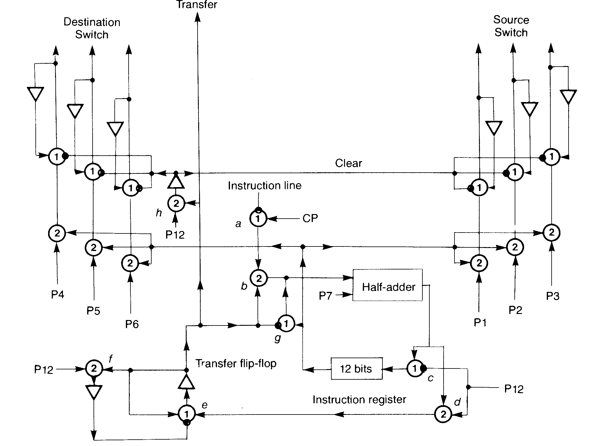
Fig. 1
The schematic is to be read as follows (see [Wilkinson1951]):
- A circle with two inputs and a
2inside is an AND Gate as it opens if all 2 inputs are active (e.g. b, d, f). - A circle with a
1inside and an inhibit input (with a small circle) passes all pulses unless the inhibit input is active, it is thus like a normally-closed switch. - A (large) triangle in flow direction is a unit delay, that reproduces the input one clock time later
- CP is the master clock pulse.
- P1, P2, upto P12 are clock pulses for the first, second etc bits of a word cycle, preferably generated by a ring counter.
In contrast to today's usage, all logic signals are represented by individual pulses that return to zero between two pulses. While this is slower than logic levels, it allows the machine to use a single clock pulse CP, instead of two non-overlapping clock pulses.
Logical signals are combined using a majority logic, hence the notation of a number in a circle that shows the threshold.
Unit delays, i.e. pulse delays for one clock time, were made of inductors and capacitors for the delay, gated with a clock pulse, see e.g. Turing's design papers for the ACE. The major disadvantage is that the system clock must be exactly matched and cannot be slowed down — which is not feasible with delay line storage anyhow.
On the left is shown the extraction of the destination port number,
and at the right for the source port number:
The bits coming out of the instruction register
are sampled at P1 to P6, and saved in flip-flops,
which are reset with P12 at the end of a transfer.
This is called a staticiser.
Using just a unit delay, a switch and a AND gate,
a very unusual D-type flip-flop with clock (AND) and
reset (switch) is made.
It would be a nice exhibit to show such a flip-flop with valves
side-by-side with a solution using transistors and diodes.
Note that modern TTL-logic (e.g. 7474) uses about 13 transistors.
The basic part of the instruction processing is the timing delay, done by the following means (small letters refer to gates in the original schematic in Fig. 1):

Fig. 2
To read the next instruction from the instruction line,
the RS flip-flop is set and the transfer signal becomes active;
and the left switch routes the negated word pulses of the next instruction into the
instruction register IR, which is a 12-bit delay line.
P12, the last clock pulse, resets the flip-flop, and the first switch
goes to the shown state again.
In this state, the bits coming out of IR go through the Adder
and are fed into IR again.
The other input of the Adder is P7, a pulse that occurs
a the time of bit 7, thus each round the timing delay
part of the instruction register IR is incremented.
At time P12, the output of the Adder is switched to the flip-flop;
described by Huskey that if there was a carry over into bit 12 of the instruction
as kept in IR, the flip-flop is set,
the Transfer signal is raised, and the bit sequence
coming from the Instr.Line is read into the IR again.
Obviously, the output of the half adder had to be inverted,
as the overflow would result in a zero bit.
(Consider 000001 as timing in the instructions word (MSB first)
changed to 111110, incremented to 111111, thus giving a 1
at P12. The next round it becomes 000000, now the zero MSB
should initiate the transfer.
Inverting the instruction effectively did change the timing delay to its negative minus one, allowing to use an adder instead of a subtractor.
As in Turing's ACE description, P1 to P12 are twelve distinct clock pulses, each one corresponding to one bit of the 12 bit word, P1 for the least significant and P12 for the most significant bit. One round of P1 to P12 is called a word (minor) cycle. After a memory (major) cycle, the bits of the long delay lines emerge again. The number of word cycles per memory cycle is not given explicitly, but a 5 bit time field indicates that the number is 32.
After power on all delay lines are empty; the instruction register can at any time be cleared by inhibiting the serial input.
For a single step mode, setting the transfer flip flop must be disabled; the pulse to set it will be repeated every second cycle.
Programming
The article mentioned gives not a single example programme, evidently because no program has been seen so far that can use the delay line for variables.
Huskey writes:
Instructions came from an instruction line the same time
that transfer occurred.
and continued:
This was very restrictive and made the system unsuitable
for general computation, but is was sufficient to illustrate
the principles.
It is nice to demonstrate the hardware, but more than restrictive, better said useless for programming.
The machine allows to execute at most 32 instructions — which is more than enough — in any order, because each instruction contains the wait time to the next.
This allows to execute a number of initialisation instructions and then a loop, e.g. to enumerate integer number sequences.
As with the ACE, the first phase in programming (preliminary coding) is to write down the instructions independent of timing, showing instructions in order of execution, using arrows and lines to show branches and loops.
Enumerating natural numbers starting a 1 then gives:
	5 ~	2       set TS to 1
	3 ~ 0 ←┐    output
	5 ~ 3 ─┘    increment TS
However, the data delay line DL is useless.
Any instruction can only access the data word at the same position,
so there is only one instruction per data word,
either to overwrite it, or to obtain its content.
(Using both, as source and destination, is obviously useless,
as it just overwrites the current word with itself.)
As no two instructions can access the same data word,
processing of data is impossible.
The most simple solution is to keep DL2 with 32 words,
but use 8 words only for DL,
so that there are 4 different instructions that could access the same data.
This is clearly weird, but the only solution known so far that does not change the overall design at all.
As an example, take the generation of triangular numbers 1, 3, 6, 10, 15, 21, 28 (OEIS A00217), in pseudocode:
	a =: 1
	a =: 1
	(
		print b
		b =+ a
		a =+ 1
	)
Let us denote the accumulator as t, and keep a and b as data words:
	1 => a
	1 => b
	(
		b => $		output
		a => t
		1 +> t		increment a
		t => a
		b +> t		new b
		t => b
	)
So there are 3 instructions to access a and 4 to access b.
Let us be a at 0, thus instructions 0,8,16,24
and b at 1, thus instructions 1,9,17,25,
the program becomes (wait implicit to reach the next line):
	 0:	5 ~ 1		1 => a
	 1:	5 ~ 1		1 => b
	 9:	1 ~ 0		b => $
	 8:	1 ~ 2		a => t
	10: 5 ~ 3		1 +> t
	16: 3 ~ 1		t => a
	17:	1 ~ 3		b +> t
	25: 2 ~ 1 :9	t => b and continue at 9
The wait times are thus:
	 0: 0
	 1: 7
	 9: 30
	 8: 1
	10: 5
	16: 0
	17: 7
	25: 15
With 6 instructions in the loop and 58 additional waits, a new number will be printed each 64 (must be multiple of 32) word cycles.
Instead to try a different allocation, a modified programme will do everything in one loop:
	1 => a
	1 => b
	1 => t
	(
		t => $
		a => t
		1 +> t		increment
		t => a
		b +> t		new b
		t => b
	)
Locations allocated and wait times added:
	 0:	5 ~ 1	0	1 => a
	 1:	5 ~ 1	0	1 => b
	 2: 5 ~ 2	0	1 => t
	 3:	3 ~ 0	4	t => $
	 8:	1 ~ 2	1	a => t
	10: 5 ~ 3	5	1 +> t
	16: 3 ~ 1	0	t => a
	17:	1 ~ 3	6	b +> t
	24: 2 ~ 1	10	t => b; goto 3
Now the inner loop has still 6 instructions, but only 26 extra delays, so that the loop requires 32 word cycles.
Program Load
Provided whatever demonstration programme is desired, it must be somewhat established into the second delay line.
In the Pilot ACE, it was not necessary — if possible at all — to key in some initial instructions, because an instruction of all zeroes reads the input to the instruction register, normally from the card reader. This first instruction executed normally reads the next 31 data words from the card reader to DL1 and continues there. Details are explained in Turing's description of the Pilot ACE.
After power on, the instruction register and all other delay lines are zero, as all recirculated pulses are lost. This can also be obtained by a reset key that inhibits recirculation.
The instruction with all zeroes reads the input dynamiciser and sends it to the output staticiser; to send it to the programme delay line would require:
0 ~ 5
If destination 0 would be exchanged with destination 5, the instruction with all zeroes, i.e.:
0 ~ 0 0
copies the bit pattern of the input dynamiciser to the current position of DL2, and executes the next instruction in DL2, which, when zero, repeats the process, until the first non-zero instruction is encountered.
If the machine is in single-step mode (see above), the contents of DL2 can be keyed in manually, or, if a some kind of reader is provided, read from that reader.
So the other proposed change over the original would be
Technical Details
Some remarks on the schematics in Fig. 1 follow:
- The buffers (flip-flops) for the destination and source switches
are cleared one unit delay after
P12andTransfer, i.e. duringP1of the following cycle, conflicting with setting the lowest bit. If the wait count is greater zero, the next cycle sets the bit finally. - Because the instruction is obtained at the same time the transfer is active, it cannot directly set the source and direction switches, as this would spoil the transfer.
- The clear signal for the transfer flip-flop is rather critical,
so that the transfer signal does not end prematurely
and truncates the data transferred,
but does not extend into
P1time and start a partial transfer. - The transfer signal is derived from the unit delay of the
transfer flip-flop, thus it correctly becomes valid at
P1time. However, the clear signal created by gatefshould not use a unit delay; as shown, the transfer flip-flop will be off duringP1and, due to the unit delay output, the transfer signal will extend intoP1. - The adder is named a half-adder.
In modern terms, a half-adder is just an XOR and AND producing sum and carry.
It is, actually, an incrementer with a carry delay not shown, where the carry
is additionally set by
P7, i.a. at the start of the wait time specification. - The instruction bits are inverted before they are shifted into the instruction register. As far as the source and destination numbers are concerned, this must be taken into account by the wiring of the switches. The wait time is effectively negated, and the change from -1 to 0 can be used as signal to start the transfer.
- The transfer flip-flop is set if the result of the adder at P12 is one. This would be correct if every instruction would have a 1 bit at the highest bit position; this is, however, not enforced when reading the instruction. If there were a 0 bit, the transfer would start immediately: Assume the last 6 bits of the instruction to be 010000 (binary, starting with the LSB). Inversion makes 101111, and incrementing it makes 011111, thus the output of the adder at P12 is 1, and the transfer started. Note that the next round without reading and instruction will yield 111111, and the third round 000000, so in this case, the transfer must start when the adder output is 0. It is better to use the carry output of the adder at P11.
- Gate c clears the 12th bit shifted into the IR, evidently to avoid the above case. However, it would only be effective after the first round, when the transfer is already started. Alternatively, gate c could be used after the instruction bits are inverted; then, in the above example, the input 010000 would become 101110, and the transfer started correctly independent of the 12th bit.
References
- Huskey1984:
- Harry D. Huskey: From ACE to the G-15. IEEE Annals of the History of Computing, Vol.6 No.4 pp.350-371 (1984). http://doi.ieeecomputersociety.org/10.1109/MAHC.1984.10047
- Huskey2005:
- H. D. Huskey: The ACE Test Assembly, the Pilot ACE, the Big ACE, and the Bendix G15. In Copeland, B. J., Alan Turing's Automatic Computing Engine, chapter 13, pages 281–295. Oxford University Press, 2005. ISBN 0-19-856593-3.
- Wilkinson1951:
- J. H. Wilkinson: Report on the Pilot Model of the Automatic Computing Engine. NPL London, 1951. Scan available online at http://www.alanturing.net/turing_archive/archive/l/l22/l22.php
- Woodger:
- Michael Woodger: The ACE simulator and the cybernetic Model. In: Alan Turing's Automatic Computing Engine, see [Huskey2005]